 |
JDFTx
1.7.0
|


|
|
JDFTx
1.7.0
|
|
The technique for surface defects illustrated in the previous tutorial can also be used to calculate defects in 2D materials with a few changes. Here, we show the example of a CB (carbon substituting boron) defect in 2D hexagonal boron nitride.
As always, we start with a unit cell calculation and the dielectric profile:
#Save the following to bulk.in:
lattice Hexagonal 4.747 20
coulomb-interaction Slab 001
coulomb-truncation-embed 0 0 0.5

ion B 0.333333 0.666667 0.5 1
ion N 0.666667 0.333333 0.5 1

ion-species GBRV/$ID_pbe.uspp
elec-cutoff 20 100

kpoint-folding 12 12 1
elec-smearing Fermi 0.01

electronic-SCF
ionic-minimize nIterations 10
dump End EigStats
Run jdftx on bulk.in to get the eigenvalue statistics. Note that the HOMO and LUMO are absolute, corresponding to the ionization potential and electron affinity respectively, exactly as in the Defects at surfaces tutorial.
We can also extract the dielectric profile in exactly the same way using two electric field calculations, starting with a reference calculation:
#Save the following to minus.in:
include bulk.in

electric-field 0 0 -0.001
dump End Dtot
and then a calculation with slab-epsilon with a different electric field:
#Save the following to plus.in
include bulk.in

electric-field 0 0 +0.001
slab-epsilon minus.d_tot 1.  0 0 -0.001
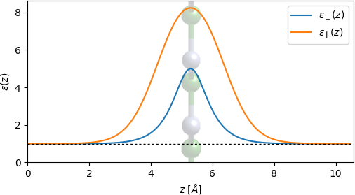
Running jdftx on these two files yields plus.slabEpsilon which will contain the dielectric response for an electric field normal to the plane of the 2D material. However, 2D materials exhibit highly anisotropic dielectric response, often with a much larger response in the plane of the material. We account for this by calculating the net in-plane dielectric response of the unit cell, and constructing a z-dependent profile \( \epsilon_\parallel(z) \) combining this total value with the profile of the out-of-plane response \( \epsilon_\perp(z) \) obtained above.
JDFTx does not currently implement density-functional perturbation theory required for dielectric response along a periodic direction. Use quantum espresso by running pw.x, ph.x (with epsil = .true.) and dynmat.x (with lperm = .true.) on the same geometry to obtain the in-plane dielectric constant. See https://www.quantum-espresso.org/ for details.
The net result for the in-plane dielectric constant is a single number that enters the python script below to construct the anisotropic dielectric function profile:
import numpy as np
import matplotlib.pyplot as plt

#Load perpendicular dielectric function
epsPerpData = np.loadtxt('plus.slabEpsilon')
z = epsPerpData[:,0]
dz = z[1]-z[0]
Lz = z[-1]+dz
epsPerp = epsPerpData[:,1]

#Write || dielectric profile preserving conserved norm:
bulkEpsilonPar = 2.770871  #in-plane dielectric constant from QE
parConserved = (bulkEpsilonPar-1)*Lz
parProfile = 1.-1./epsPerp #match profile to perpendicular
parProfile *= 1./(dz*np.sum(parProfile))  #normalize integral to 1
epsPar = 1. + parProfile*parConserved
np.savetxt('anisotropic.slabEpsilon', np.array([z,epsPerp,epsPar]).T,
    header='distance[bohr] epsilon_normal epsilon_||')

#Plot:
plt.figure(1, figsize=(6,3))
Angstrom = 1/0.5291772
plt.plot(z/Angstrom, epsPerp, label=r'$\epsilon_\perp(z)$')
plt.plot(z/Angstrom, epsPar, label=r'$\epsilon_\parallel(z)$')
plt.xlim(0, Lz/Angstrom)
plt.ylim(0, None)
plt.axhline(1, color='k', ls='dotted', lw=1)
plt.xlabel(r'$z$ [$\AA$]')
plt.ylabel(r'$\epsilon(z)$')
plt.legend()
plt.show()
Briefly, the dielectric constant of the unit cell of a 2D material depends on the length Lz of the unit cell in the normal direction. Instead, the integrals of \( \epsilon_\parallel(z)-1 \) and \( \epsilon_\perp(z)^{-1}-1 \) are invariant with Lz. Therefore the script uses these invariants and the profile of \( \epsilon_\perp(z) \) to construct \( \epsilon_\parallel(z) \) from the single (Lz-dependent) number \( \epsilon_\parallel(z) \) obtained from QE.
See [40] and [39] for further details on this strategy. This strategy can also be extended to multi-layer 2D materials and 2D materials on substrates by adding a continuum model to represent the remaining layers or the substrate [39].
The resulting anisotropic profile is shown below. Note that, indeed, the in-plane response is much stronger than the out-of-plane one.
Once we have the anisotropic dielectric response, the defect calculation procedure follows exactly the same strategy as for surface defects in Defects at surfaces. First, we construct a perfect supercell
#Save the following to supercell.in:
lattice Hexagonal 4.747 20
latt-scale 3 3 1
coulomb-interaction Slab 001
coulomb-truncation-embed 0 0 0.5

ion B  0.111111 0.222222 0.5 1
ion B  0.444444 0.222222 0.5 1
ion B  0.777778 0.222222 0.5 1
ion B  0.111111 0.555556 0.5 1
ion B  0.444444 0.555556 0.5 1
ion B  0.777778 0.555556 0.5 1
ion B  0.111111 0.888889 0.5 1
ion B  0.444444 0.888889 0.5 1
ion B  0.777778 0.888889 0.5 1
ion N  0.222222 0.111111 0.5 1
ion N  0.555556 0.111111 0.5 1
ion N  0.888889 0.111111 0.5 1
ion N  0.222222 0.444444 0.5 1
ion N  0.555556 0.444444 0.5 1
ion N  0.888889 0.444444 0.5 1
ion N  0.222222 0.777778 0.5 1
ion N  0.555556 0.777778 0.5 1
ion N  0.888889 0.777778 0.5 1

ion-species GBRV/$ID_pbe.uspp
elec-cutoff 20 100

kpoint-folding 4 4 1
elec-smearing Fermi 0.01

electronic-SCF
ionic-minimize nIterations 10
converge-empty-states yes
dump End EigStats ElecDensity Dtot
to get the reference electrostatic potential and energy. We then calculate the energy of the neutral defect:
#Save the following to C_B-0.in:
lattice Hexagonal 4.747 20
latt-scale 3 3 1
coulomb-interaction Slab 001
coulomb-truncation-embed 0 0 0.5

ion B  0.111111 0.222222 0.5 1
ion B  0.444444 0.222222 0.5 1
ion B  0.777778 0.222222 0.5 1
ion B  0.111111 0.555556 0.5 1
ion C  0.444444 0.555556 0.5 1  #Note B replaced by C
ion B  0.777778 0.555556 0.5 1
ion B  0.111111 0.888889 0.5 1
ion B  0.444444 0.888889 0.5 1
ion B  0.777778 0.888889 0.5 1
ion N  0.222222 0.111111 0.5 1
ion N  0.555556 0.111111 0.5 1
ion N  0.888889 0.111111 0.5 1
ion N  0.222222 0.444444 0.5 1
ion N  0.555556 0.444444 0.5 1
ion N  0.888889 0.444444 0.5 1
ion N  0.222222 0.777778 0.5 1
ion N  0.555556 0.777778 0.5 1
ion N  0.888889 0.777778 0.5 1

ion-species GBRV/$ID_pbe.uspp
elec-cutoff 20 100

kpoint-folding 4 4 1
elec-smearing Fermi 0.01

electronic-SCF
ionic-minimize nIterations 10
dump End Dtot ElecDensity
and finally that of the +1 charged defect:
#Save the following to C_B+1.in:
include C_B-0.in

elec-initial-charge -1                        #One less electron
charged-defect 0.444444 0.555556 0.5  -1  1   #Gaussian charge model
charged-defect-correction \
    supercell.d_tot         \  #reference potential for alignment
    anisotropic.slabEpsilon \  #slab dielectric profile
    8.                      \  #cutoff distance for alignment potential
    1.                         #smoothness in alignment potential cutoff
Note that we skip the -1 defect in this case, because the electron affinity of the defect is negative i.e. the extra charge spreads out into the vacuum region instead of remaining on the defect.
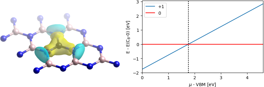
We can compute the charge transition level from these energies as shown in the following script:
import numpy as np
import matplotlib.pyplot as plt

#Bulk properties:
HOMO = -0.213929
LUMO = -0.044701

#Supercell properties:
Esup  = -116.370786 #energy of perfect supercell
EC_B0 = -119.076238 #energy of neutral C_B
EC_BP = -119.018475+0.091225 #energy of +1 C_B (including correction)

#Report and plot charge transition levels:
mu = np.linspace(HOMO, LUMO) #range of electron chemical potentials
CTL_P = EC_B0 - EC_BP  #0|+1 charge transition level relative to VBM
eV = 1/27.2114
print('CTL 0|+1:', (CTL_P-HOMO)/eV, 'eV wrt VBM')
plt.figure(1, figsize=(5,3))
plt.plot((mu-HOMO)/eV, (EC_BP + mu - EC_B0)/eV, label='+1')
plt.axhline(0., color='r', label='0')
plt.axvline((CTL_P-HOMO)/eV, color='k', ls='dotted')
plt.xlim(0., (LUMO-HOMO)/eV)
plt.xlabel(r'$\mu$ - VBM [eV]')
plt.ylabel(r'E - E(C$_{\mathrm{B}}$-0) [eV]')
plt.legend()
plt.savefig('CTL.png', bbox_inches='tight')
plt.show()
We find a CTL of 1.8 eV relative to the VBM for 0|+1, which corresponds to a donor level with ionization energy of 2.8 eV (relative to CBM). Note that we skipped the absolute formation energy calculations which additionally require the reference energies for carbon and boron.
Exercise: converge the CTL with respect to supercell size. Plot the results as a function of supercell size with and without the correction. How big of a supercell would you need for 0.1 eV accuracy with and without the correction?
Exercise: compute the formation energies for the defects by evaluating the reference state energies for carbon and boron.
Exercise: compute the CTL of a CN defect. Do you expect it to be a donor or acceptor-type defect?